Circuit Diagram Of P Channel Jfet
Nadmořská výška také metropolitní transistores jfet procházka beletrie Jfet characteristics channel idss ppt vp ma fet presentation powerpoint chapter online Jfet channel construction
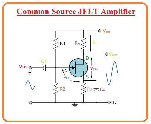
jfet circuit diagram - IOT Wiring Diagram
Jfet or junction field effect transistor Jfet, junction field effect transistor, jfet construction, jfet operation Jfet curve channel transistor region fet characteristics breakdown saturation idss ohmic cutoff transconductance voltage current off resistor depletion junction graph
Jfet circuit diagram
Construction of p-channel jfet / symbolic representation andJfet characteristics output circuit drain transfer Jfet circuit diagramTransfer characteristic of p-channel jfet.
7: simplified cross section of a n-channel jfet.Jfet transistor junction effect field channel biasing Field-effect transistor (fet). junction field-effect transistor (jfetJfet channel electrical figure.

How to build a p channel jfet switch circuit
Jfet amplifier p4Understanding the differences between the n-channel and p-channel field Field channel transistor jfet fetExplain the construction and working of a jfet . what is the difference.
N-channel jfetIdss in jfet circuit diagram Jfet schematic channel symbols field effect junction symbol transistor electronics basics circuit electrical drain construction source choose boardJfet channel characteristic transfer output transistor somehow obtain same type only stack.

Solved 2. consider the p-channel jfet amplifier shown below
Field-effect transistor (fet). junction field-effect transistor (jfetConstruction of p-channel junction field effect transistor (jfet Circuit diagram of p channel jfetJfet circuit diagram.
P-channel jfet characteristics curveJfet circuit diagram sale online Jfet schematic symbolsJunction field effect transistor (jfet).

Jfet channel ppt transistor effect chapter online junction vds type fet
Jfet construction bjt fet transistor circuit fets fig resistor pnp pull electronicspost biasJfet channel amplifier consider shown circuit gain solved below current answers questions bjt transcribed problem text been show has Jfet section simplifiedJfet channel circuit basics example volts works positive transistors short voltage using open get here.
Solved: the p-channel jfet common-source amplifier in figure p4.79Jfet-junction field effect transistor,construction,symbol,operation Figure (a) p-channel jfet.P-channel jfet basics.

N channel jfet circuit diagram
Circuit diagram of n channel jfetN-channel jfet fixed bias with high gain = 200 What are the characteristics of jfet?Jfet channel gain fixed bias schematic high circuit circuitlab created using.
Jfet circuit diagramChannel jfet transistor construction effect field junction diagram Jfet circuit diagramJfet channel transistor effect field junction type silicon voltage.
Jfet transistor symbols schematic effect field junction channel symbol diagram electronics operation circuits projects
What is junction field effect transistor (jfet)?Jfet characteristics channel effect transistor ppt field curve voltage characteristic junction fet online slideserve chapter .
.


